Home > Press > HKUST researchers develop a novel integration scheme for efficient coupling between III-V and silicon
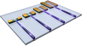 |
High-performance Si-waveguide coupled III-V photodetectors grown on SOI CREDIT
Credit: The Hong Kong University of Science and Technology |
Abstract:
Researchers at the Hong Kong University of Science and Technology (HKUST) has recently developed a novel integration scheme for efficient coupling between III-V compound semiconductor devices and silicon components on silicon photonics (Si-photonics) platform by selective direct epitaxy, unlocking the potential of integrating energy-efficient photonics with cost-effective electronics, as well as enabling the next generation telecommunications with low cost, high speed and large capacity.
HKUST researchers develop a novel integration scheme for efficient coupling between III-V and silicon
Hong Kong, China | Posted on November 18th, 2022
Over the past few years, data traffic has been growing exponentially driven by various applications and emerging techniques such as big data, automobiles, cloud applications and sensors. To address the issues, Si-photonics has been widely investigated as a core technology to enable, extend, and increase data transmission through energy-efficient, high-capacity and low-cost optical interconnects. While silicon-based passive components have been well established on Si-photonics platform, the lasers and photodetectors can’t be realized by silicon and necessitate the integration of other materials such as III-V compound semiconductors on silicon.
III-V lasers and photodetectors on silicon has been investigated by two main methods. The first one is the bonding-based method which has yielded devices with impressive performance. However, it requires complicated manufacturing technique that is low yield and high-cost, making mass production very challenging. The other way is direct epitaxy method by growing multiple layers of III-V on silicon. While it provides a solution with lower cost, larger scalability and higher integration density, the micrometers thick III-V buffer layers which are crucial for this method hinders efficient light coupling between III-V and silicon – the key for integrated Si-photonics.
To address these issues, the team led by Prof. Kei-May LAU, Professor Emeritus of the Department of Electronic and Computer Engineering at Hong Kong University of Science and Technology (HKUST), developed lateral aspect ratio trapping (LART) – a novel selective direct epitaxy method that can selectively grow III-V materials on silicon-on-insulator (SOI) in a lateral direction without the need of thick buffers. Furthermore, based on this novel technology, the team devised and demonstrated unique in-plane integration of III-V photodetectors and silicon elements with high coupling efficiency between III-V and silicon. Compared to the commercial ones, the performance of photodetectors by such approach is less noisy, more sensitive, and has wider operation range, with record-high speed of over 112 Gb/s – way faster than existing products. For the first time, the III-V devices can be efficiently coupled with Si elements by direct epitaxy. The integration strategy can be easily applied to the integration of various III-V devices and Si-based components, thereby enabling the ultimate goal of integrating photonics with electronics on silicon photonics platform for data communications.
“This was made possible by our latest development of a novel growth technique named lateral aspect ratio trapping (LART) and our unique design of coupling strategy on the SOI platform. Our team’s combined expertise and insights into both device physics and growth mechanisms allow us to accomplish the challenging task of efficient coupling between III-V and Si and cross-correlated analysis of epitaxial growth and device performance,” said Prof. Lau.
“This work will provide practical solutions for photonic integrated circuits and fully integrated Si-photonics, light coupling between III-V lasers and Si components can be realized through this method” said Dr. Ying Xue, first author of the study.
This is a collaborative work with a research team led by Prof. Hon Ki Tsang of Department of Electronic Engineering at Chinese University of Hong Kong (CUHK) and a research team led by Prof. Xinlun Cai of School of Electronics and Information Technology at Sun Yat-sen University (SYSU). The device fabrication technology in the work was developed at HKUST’s Nanosystem Fabrication Facility (NFF) on Clear Water Bay campus. The work is supported by Research Grants Council of Hong Kong and Innovation Technology Fund of Hong Kong. This work has recently been published in Optica.
####
For more information, please click here
Contacts:
Chun-ki WONG
Hong Kong University of Science and Technology
Office: 852-346-92512
Copyright © Hong Kong University of Science and Technology
If you have a comment, please Contact us.
Issuers of news releases, not 7th Wave, Inc. or Nanotechnology Now, are solely responsible for the accuracy of the content.
Bookmark:


 ARTICLE TITLE
News and information
Researchers at Purdue unlock light-matter interactions on sub-nanometer scales, leading to ‘picophotonics’ November 18th, 2022
Rice turns asphaltene into graphene for composites: ‘Flashed’ byproduct of crude oil could bolster materials, polymer inks November 18th, 2022
How “2D” materials expand: New technique that accurately measures how atom-thin materials expand when heated could help engineers develop faster, more powerful electronic devices November 18th, 2022
New insights into energy loss open doors for one up-and-coming solar tech November 18th, 2022
Wireless/telecommunications/RF/Antennas/Microwaves
Synthesis of air-stable room-temperature van der Waals magnetic thin flakes September 30th, 2022
Quantum network nodes with warm atoms June 24th, 2022
Photonic integrated erbium doped amplifiers reach commercial performance: Boosting light power revolutionizes communications and autopilots June 17th, 2022
Nanoscale bowtie antenna under optical and electrical excitations June 3rd, 2022
Possible Futures
NIST’s grid of quantum islands could reveal secrets for powerful technologies November 18th, 2022
A new experiment pushes the boundaries of our understanding of topological quantum matter: The behavior of bosonic particles observed in a magnetic insulator fabricated from ruthenium chloride can be explained by a relatively new and little-studied physics phenomenon called the B November 18th, 2022
Trial by wind: Testing the heat resistance of carbon fiber-reinforced ultra-high-temperature ceramic matrix composites: Researchers use an arc-wind tunnel to test the heat resistance of carbon fiber reinforced ultra-high-temperature ceramic matrix composites November 18th, 2022
New insights into energy loss open doors for one up-and-coming solar tech November 18th, 2022
Discoveries
An on-chip time-lens generates ultrafast pulses: New device opens the doors to applications in communication, quantum computing, astronomy November 18th, 2022
Researchers at Purdue unlock light-matter interactions on sub-nanometer scales, leading to ‘picophotonics’ November 18th, 2022
Rice turns asphaltene into graphene for composites: ‘Flashed’ byproduct of crude oil could bolster materials, polymer inks November 18th, 2022
How “2D” materials expand: New technique that accurately measures how atom-thin materials expand when heated could help engineers develop faster, more powerful electronic devices November 18th, 2022
Announcements
NIST’s grid of quantum islands could reveal secrets for powerful technologies November 18th, 2022
A new experiment pushes the boundaries of our understanding of topological quantum matter: The behavior of bosonic particles observed in a magnetic insulator fabricated from ruthenium chloride can be explained by a relatively new and little-studied physics phenomenon called the B November 18th, 2022
How “2D” materials expand: New technique that accurately measures how atom-thin materials expand when heated could help engineers develop faster, more powerful electronic devices November 18th, 2022
New insights into energy loss open doors for one up-and-coming solar tech November 18th, 2022
Interviews/Book Reviews/Essays/Reports/Podcasts/Journals/White papers/Posters
An on-chip time-lens generates ultrafast pulses: New device opens the doors to applications in communication, quantum computing, astronomy November 18th, 2022
Researchers at Purdue unlock light-matter interactions on sub-nanometer scales, leading to ‘picophotonics’ November 18th, 2022
Rice turns asphaltene into graphene for composites: ‘Flashed’ byproduct of crude oil could bolster materials, polymer inks November 18th, 2022
How “2D” materials expand: New technique that accurately measures how atom-thin materials expand when heated could help engineers develop faster, more powerful electronic devices November 18th, 2022
Photonics/Optics/Lasers
An on-chip time-lens generates ultrafast pulses: New device opens the doors to applications in communication, quantum computing, astronomy November 18th, 2022
Researchers at Purdue unlock light-matter interactions on sub-nanometer scales, leading to ‘picophotonics’ November 18th, 2022
Semi-nonlinear etchless lithium niobate waveguide with bound states in the continuum November 4th, 2022
Spin photonics to move forward with new anapole probe November 4th, 2022
- Coinsmart. Europe’s Best Bitcoin and Crypto Exchange.Click Here
- Platoblockchain. Web3 Metaverse Intelligence. Knowledge Amplified. Access Here.
- Source: http://www.nanotech-now.com/news.cgi?story_id=57250
HKUST researchers develop a novel integration scheme for efficient coupling between III-V and silicon
Republished By Plato
Home > Press > HKUST researchers develop a novel integration scheme for efficient coupling between III-V and silicon
Credit: The Hong Kong University of Science and Technology
Abstract:
Researchers at the Hong Kong University of Science and Technology (HKUST) has recently developed a novel integration scheme for efficient coupling between III-V compound semiconductor devices and silicon components on silicon photonics (Si-photonics) platform by selective direct epitaxy, unlocking the potential of integrating energy-efficient photonics with cost-effective electronics, as well as enabling the next generation telecommunications with low cost, high speed and large capacity.
HKUST researchers develop a novel integration scheme for efficient coupling between III-V and silicon
Hong Kong, China | Posted on November 18th, 2022
Over the past few years, data traffic has been growing exponentially driven by various applications and emerging techniques such as big data, automobiles, cloud applications and sensors. To address the issues, Si-photonics has been widely investigated as a core technology to enable, extend, and increase data transmission through energy-efficient, high-capacity and low-cost optical interconnects. While silicon-based passive components have been well established on Si-photonics platform, the lasers and photodetectors can’t be realized by silicon and necessitate the integration of other materials such as III-V compound semiconductors on silicon.
III-V lasers and photodetectors on silicon has been investigated by two main methods. The first one is the bonding-based method which has yielded devices with impressive performance. However, it requires complicated manufacturing technique that is low yield and high-cost, making mass production very challenging. The other way is direct epitaxy method by growing multiple layers of III-V on silicon. While it provides a solution with lower cost, larger scalability and higher integration density, the micrometers thick III-V buffer layers which are crucial for this method hinders efficient light coupling between III-V and silicon – the key for integrated Si-photonics.
To address these issues, the team led by Prof. Kei-May LAU, Professor Emeritus of the Department of Electronic and Computer Engineering at Hong Kong University of Science and Technology (HKUST), developed lateral aspect ratio trapping (LART) – a novel selective direct epitaxy method that can selectively grow III-V materials on silicon-on-insulator (SOI) in a lateral direction without the need of thick buffers. Furthermore, based on this novel technology, the team devised and demonstrated unique in-plane integration of III-V photodetectors and silicon elements with high coupling efficiency between III-V and silicon. Compared to the commercial ones, the performance of photodetectors by such approach is less noisy, more sensitive, and has wider operation range, with record-high speed of over 112 Gb/s – way faster than existing products. For the first time, the III-V devices can be efficiently coupled with Si elements by direct epitaxy. The integration strategy can be easily applied to the integration of various III-V devices and Si-based components, thereby enabling the ultimate goal of integrating photonics with electronics on silicon photonics platform for data communications.
“This was made possible by our latest development of a novel growth technique named lateral aspect ratio trapping (LART) and our unique design of coupling strategy on the SOI platform. Our team’s combined expertise and insights into both device physics and growth mechanisms allow us to accomplish the challenging task of efficient coupling between III-V and Si and cross-correlated analysis of epitaxial growth and device performance,” said Prof. Lau.
“This work will provide practical solutions for photonic integrated circuits and fully integrated Si-photonics, light coupling between III-V lasers and Si components can be realized through this method” said Dr. Ying Xue, first author of the study.
This is a collaborative work with a research team led by Prof. Hon Ki Tsang of Department of Electronic Engineering at Chinese University of Hong Kong (CUHK) and a research team led by Prof. Xinlun Cai of School of Electronics and Information Technology at Sun Yat-sen University (SYSU). The device fabrication technology in the work was developed at HKUST’s Nanosystem Fabrication Facility (NFF) on Clear Water Bay campus. The work is supported by Research Grants Council of Hong Kong and Innovation Technology Fund of Hong Kong. This work has recently been published in Optica.
####
For more information, please click here
Contacts:
Chun-ki WONG
Hong Kong University of Science and Technology
Office: 852-346-92512
Copyright © Hong Kong University of Science and Technology
If you have a comment, please Contact us.
Issuers of news releases, not 7th Wave, Inc. or Nanotechnology Now, are solely responsible for the accuracy of the content.
Bookmark:


News and information
Wireless/telecommunications/RF/Antennas/Microwaves
Possible Futures
Discoveries
Announcements
Interviews/Book Reviews/Essays/Reports/Podcasts/Journals/White papers/Posters
Photonics/Optics/Lasers
2023-24 Round 2 Race Offence No 22 – Car 79
Centralized crypto exchanges see $2 trillion surge in trading volumes in Q1: CoinGecko
Lakers Remain Without Reinforcements After Optimism of a Game 3 Return
Top 10 Reasons to Attend Blockchain Futurist Conference – CryptoCurrencyWire
Bloomberg: Reasons Behind Bitcoin Traders’ Waning Bullishness
Bitcoin Price Recovery Is Halted At $68,000 As It Continues To Fall
Emerging Trends in RWA Tokenization: Bridging the Digital and Physical
Quantum News Briefs: April 25, 2024: News From the European Commission • NIST • Exail and Lawrence Livermore National Laboratory • Oxford Instruments and the University of Bristol – Inside Quantum Technology
Synchronous source and measure system takes a modular approach to low-level measurement – Physics World