
In a number of solid-state systems, the quantum Hall effect (QHE) is found to demonstrate topologically protected dissipation less edge channels with their transversal conductance quantized by e2/h, where e and h are the elementary charge and the Planck constant, respectively1,2,3,4,5. This peculiar behaviour is crucial, for example, in the implementation of quantum-based-resistance standards with an extremely high precision and reproducibility6. Among the few known systems that manifest QHE, graphene receives special attention for its distinct band structure and the resulting Nth Landau level (LL) at the energy of ({varepsilon }_{{{{rm{LL}}}}}(N)={{{rm{sgn}}}}(N){v}_{{rm{F}}}sqrt{2ehslash B| N| }) under magnetic field B, where vF is the Fermi velocity7,8,9 and the Landau quantization of graphene in the parameter space of B and n is defined as the famed Landau fan, with all LLs linearly extrapolated to the charge neutrality point (CNP)8,9,10.
Interfacial coupling is known to affect the QHE in graphene, usually in two different ways: charge impurities that cause a reduced mobility yet a wider quantum Hall (QH) plateaux in some circumstances6, and charge transfer that, to some extent, shifts the effective doping11,12,13,14,15,16. Theories predict that the interplay between an antiferromagnetic insulator and graphene can give rise to topological quantum ground states, such as quantum anomalous Hall phases17,18,19. Experimentally, RuCl3/graphene is, indeed, spotted with a strong charge transfer, which is sometimes possibly coupled to the magnetism20 and sometimes not fully evidenced so21.
In this work, we investigate the case of monolayer graphene interfaced with CrOCl, an antiferromagnetic insulator. By examining multiple configurations of graphene encapsulated with hexagonal boron nitride (h-BN) and/or CrOCl, we mapped out the peculiar interfacial coupling between the carbon honeycomb lattice and CrOCl in the parameter space of temperature T, total gate doping ntot, magnetic field B and displacement field D. At low temperatures, at which the CrOCl bulk was totally insulating, a strong interfacial coupling (SIC) was found in certain gate ranges. At finite magnetic fields, this led to a gate-tunable crossover from fan-like to cascades-like Landau quantization. In the SIC regime, a QHE phase with parabolic dependence between B and D was obtained in a wide effective doping range from 0 to 1013 cm−2, with a Landau quantization of a ν = ±2 plateau starting from as low as sub-100 mT at 3 K, and remained quantized at ~350 mT at 80 K.
Monolayered graphene, thin CrOCl flakes and encapsulating h-BN flakes were exfoliated from high-quality bulk crystals and stacked in ambient conditions using a dry transfer method22. The van der Waals heterostructures were then patterned into Hall bars with their electrodes edge contacted. As seen in Fig. 1a, the field-effect curve of h-BN–graphene–CrOCl samples (red curve) differs from the conventional h-BN–graphene–h-BN ones (blue curve), with the resistive Dirac peak disappearing and a degraded gate tunability (the configurations are illustrated in the Fig. 1a insets). Figure 1b shows the crystal structure of CrOCl (ref. 23). We first started with single-gated devices and found that an SIC took place and affected the actual doping in graphene, which exhibited a drastic discrepancy with the doping expected from a conventional gate dielectric, as shown in Supplementary Figs. 1–6.
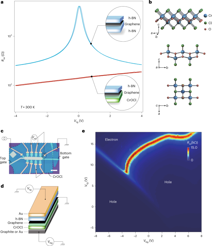
a, Field effect curves of graphene encapsulated with h-BN and/or CrOCl. Insets: schematic configurations. b, Schematics of the crystallographic structure of CrOCl. c,d, Optical micrograph image of a typical h-BN–graphene–CrOCl sample (c), illustrated in d. Scale bar, 5 μm. e, Colour map of a dual gate scan of the field effect in a typical sample, measured at a temperature of T = 3 K and a magnetic field of B = 0.
Figure 1c shows the optical image of a typical h-BN–graphene–CrOCl device, with its structure illustrated in Fig. 1d. A dual-gate mapping of the resistance obtained at T =3 K is given in Fig. 1e. Three notable regions are seen, each separated by a resistive peak and marked as either hole or electron doping, as determined by measurements at high magnetic fields discussed below. To further elucidate the SIC in the current system, we define the effective displacement field as Deff = (CtgVtg − CbgVbg)/2ϵ0 − D0, and the induced total carrier of the two gates as ntot = (CtgVtg + CbgVbg)/e − n0, as commonly used in dual-gated graphene devices24,25. Here, Ctg and Cbg are the top and bottom gate capacitances per area, respectively, and Vtg and Vbg are the top and bottom gate voltages, respectively. n0 and D0 are the residual doping and residual displacement field, respectively. Notice that the real doping in graphene ngraphene can be affected by the interfacial states of CrOCl, whose carrier density is defined as n2 (Supplementary Note 1), and therefore different from ntot in the SIC phase, as is discussed later. Examples of dual-gated maps of channel resistance in the Deff–ntot space are given in Supplementary Figs. 7–12.
Figure 2a shows a magnetic field scan of Rxy along a fixed carrier density at the hole side with ntot ≈ −3.8 × 1012 cm−2 (red dashed line in Fig. 2b, a mapping of the channel resistance of device-S16 in the Deff−ntot space). Little Deff dependence of the filling fraction (that is, LLs) is seen. This is the standard behaviour of monolayer graphene, as there is no z dimension and thus the displacement field plays no role in the LLs. Strikingly, as shown in Fig. 2c, a magnetic field scan of transverse resistance Rxy along ntot ≈ + 1.8 × 1012 cm−2 (green dashed line in Fig. 2b) exhibits drastically different patterns as compared with that in Fig. 2a. More details of the carrier types in the dual-gated devices are given in Supplementary Fig. 13. This, as in Fig. 2c, allows one to reach the electron side at Deff ≈ 0.8 V nm–1, as indicated by the line profiles of both Rxx and Rxy at 12 T in Fig. 2d. In this regime (we call it the SIC–QHE phase), Rxy is quantized in an extremely wide parameter space. For example, at B = 14 T, a filling fraction of ν = ±2 is found in the effective doping of ntot from 0 to 1013 cm−2 with a displacement field difference δD of over ~2 V nm–1, which converts into a very large range of gate voltages.
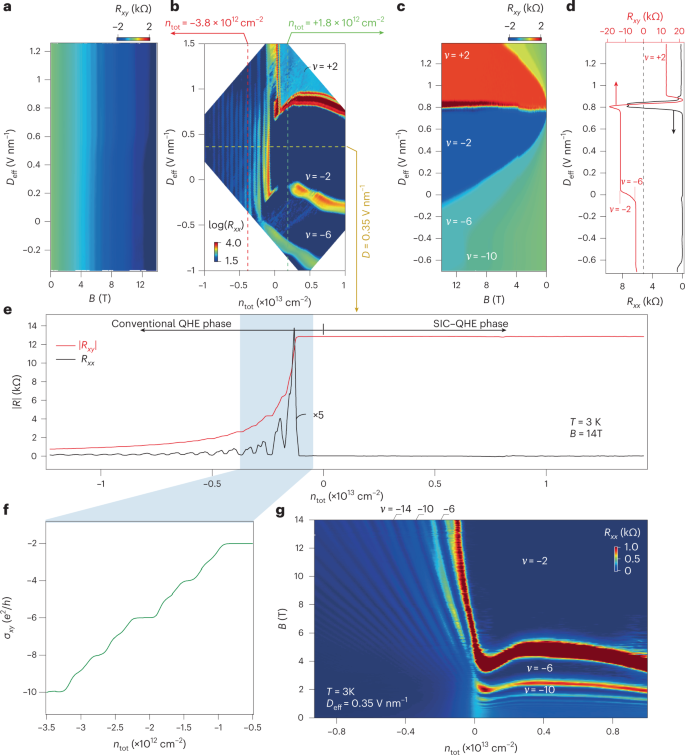
a,c, Colour maps of Rxy as a function of B, recorded along the red (a) and green (c) dashed lines in b. b, Rxx in the parameter space of Deff and ntot, measured at 14 T and 3 K. d, Line profiles of Rxx and Rxy at B = 12 T in c. e,f, Line profiles along the yellow dashed lines in b of Rxx and Rxy at Deff = 0.35 V nm–1 (e), with the zoomed-in σxy shown in f. g, Gate-tunable crossover from fan-like to cascade-like Landau quantization at Deff = 0.35 V nm–1.
Figure 2e shows the line profiles of Rxx and Rxy at Deff = 0.35 V nm–1 (along the yellow dashed line in Fig. 2b) at B = 14 T and T = 3 K. It is seen that on the hole side (noted as the conventional QHE phase), Landau quantizations are in agreement with those observed in conventional monolayered graphene8,9. Full degeneracy lifting with each integer filling fractions from ν = –2 to –10 is seen in the zoomed-in window in Fig. 2f. By fitting the hole-side effect curve at a zero magnetic field (Supplementary Fig. 14), the hole carrier mobility was estimated to be about 104 cm2 V−1 s−1. On the positive side of ntot in Fig. 2e, the SIC–QHE phase dominated, as the QH plateau of ν = –2 extended throughout the whole gate range. By varying the magnetic fields at D = 0.35 V nm−1, we obtained a colour map in the parameter space of B and ntot, shown in Fig. 2g. It is seen that the SIC led to a change in Landau quantization from the well-known fan-like behaviour to a cascade-like one. To verify ngraphene as compared with ntot in the sample, we extracted neff from the Hall resistance at low fields (that is, B < 0.5 T before the quantum oscillation started)—Fig. 2g shows a slope of ~1 with ntot at the conventional phase, but a strong departure at a positive ntot, as shown in Supplementary Fig. 15. Moreover, to have a global picture of the major features described above, the colour maps shown in Fig. 2 were replotted in a three-dimensional presentation, as shown in Supplementary Fig. 16. All these observations were reproducible in multiple samples (Supplementary Figs. 17 and 18), and also confirmed in samples fabricated in a glove box, which ruled out defects in graphene–CrOCl heterostructures (Supplementary Fig. 19).
The central result of this article is the observation of an SIC–QHE phase, in which Landau quantizations seem to be ‘pinned’, such as shown in Fig. 2g. A trivial explanation for this would be that the charge accumulation at the interface of graphene–CrOCl screened the positive gate voltages applied, which leads to a failure of electron injection. However, as shown in Fig. 2c, Deff totally shuffles the LLs (hence the ngraphene), which rules out the ‘charge pinning’ picture, as it would then be D independent, as in the conventional QHE phase (such as in Fig. 2a). Moreover, the Landau quantization seemed to approach the B = 0 limit in the SIC–QHE phase, as shown in Fig. 2c.
To further clarify this perplexing scenario, we carried out a zoomed-in scan of the low magnetic field part of Fig. 2c. We defined the displacement field in which the carrier type switches from holes to electrons as Dneutral, and thus the D axis was renormalized as δD = D − Dneutral. As shown in Fig. 3a,b (Rxx and Rxy, respectively), wide Landau plateaux are seen. The quantized regions touch the B = 0 T line, and a tiny width still exists in the vicinity of a zero magnetic field. The D–B relation of LLs observed here is distinct from those found in other multilayered graphene systems26,27,28. We took the δD = –0.08 V nm–1 here (indicated by the white dashed line in Fig. 3b), and plotted both Rxx and Rxy (Fig. 3c). The curves show a well-quantized plateaux of Rxy= ± 0.5h/e2 starting from B as low as sub-100 mT, at which Rxx shows near-zero reminiscent values at each plateau. Although a quantum anomalous Hall effect (QAHE) or Chern insulator is claimed in graphene systems29,30,31,32, our device with a h-BN–monolayer-graphene–CrOCl heterostructure seems to be topologically trivial when a magnetic field is completely absent, and the observed Rxy quantization at a very low B is still in the regime of QH states, as the quantization of ν = ± 2 is inherited from the Dirac electrons, and no magnetic hysteresis (that is, the coercive field) is seen in the trace–retrace loop of a magnetic scan in our system (indicated by arrows in Fig. 3c, and see Supplementary Fig. 20). More discussion can be seen in Supplementary Note 2. A trivial effect of gate leakage was ruled out, and multiple samples were tested to a maximum temperature before gate leakage took place, shown in Supplementary Figs. 21–23. Notably, this robust SIC–QHE phase in the graphene/CrOCl heterostructure prevails at much higher temperatures (Fig. 3c inset).
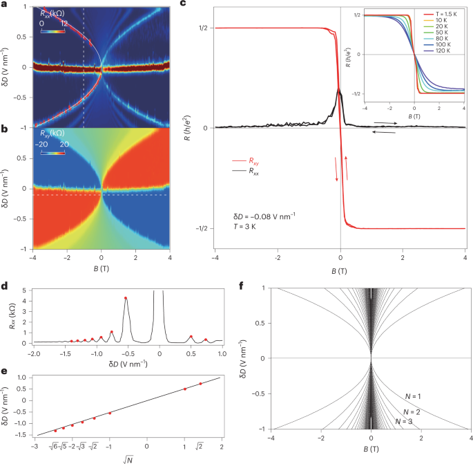
a,b, Rxx (a) and Rxy (b) of device-S16 plotted in the parameter space of δD and B. c, Line profiles of Rxx and Rxy at δD = –0.08 V nm–1. Inset: temperature dependence of another typical sample (device-S40) at δD = –0.15 V nm–1. d, Line profile of Rxx in a at B = –1 T (indicated by the vertical white dashed line). Red dots are resistive peaks picked by each maximum. e, Dependence of δD and (sqrt{N}). The black solid line is a linear fit. f, Parabolic dependence of (updelta D=alpha sqrt{B|N| }), plotted with α = 0.513 and ∣N∣ < 200.
By extracting a line profile of Rxx in Fig. 3a at B = –1 T (indicated by the vertical white dashed line), resistive peaks were found at each LL, as indicated by the red dots in Fig. 3d. It was found that the δD values at each resistive peak were in linear dependence with (sqrt{N}), with N the Nth LL, shown in Fig. 3e. This is a typical Landau quantization energy dependence in conventional monolayered graphene. Indeed, the δD–B relation can be fitted using a parabolic curve as (updelta D=alpha sqrt{B| N| }). The peaks of Rxx of the first LL in Fig. 3a (red circles) were fitted with a white solid parabolic curve, with α = 0.513. The first 200 LLs were then plotted (Fig. 3f), and well simulated the experimental δD data. This indicates that δD linearly tunes the chemical potential of the LLs of graphene, which stimulated us to propose a possible mechanism to explain the SIC–QHE as outlined in the following section. Interestingly, the observed SIC–QHE phase seems to have no connection to the antiferromagnetic nature of CrOCl, as its Néel temperature is ~13 K (ref. 23), much lower than the upper bound temperature for the SIC–QHE phase. In addition, we noticed that a sister compound of CrOCl, FeOCl, is far less stable, and could not be used to check the universality of the findings in this work (Supplementary Fig. 24).
We then replotted (Fig. 4a) the Rxx of device-S16 in the Deff–ntot space at 14 T with false colour that separates the boundary between the conventional and SIC phases, and the LLs naturally denote iso-doping lines, as defined by ν = hngraphene/eB. Two key features are seen in Fig. 4a. First, the CNP is bent as the system enters from conventional phase into the SIC phase. Second, each spacing between the iso-doping lines increases as the system enters deeper into the SIC phase. We propose an electrostatic model in Supplementary Note 1. An interfacial band with considerable charge density of n2 is introduced at the surface of CrOCl with a distance d2 below the graphene layer, and the top and bottom gates are located at distances d1 and d3, respectively, as illustrated in Supplementary Fig. 25a,b. By evaluating the model, we found that these two major features can be well reproduced, as shown in the phase diagram in Fig. 4b. Nevertheless, in the simplified model we had to introduce two assumptions—a band structure reconstruction with an enhanced Fermi velocity once the Fermi level of graphene becomes aligned with the interfacial band in CrOCl, and also that the interfacial band exhibits no contribution to transport, as discussed in Supplementary Figs. 25–28.
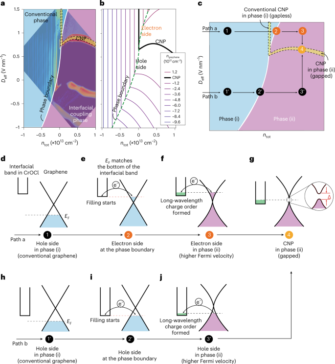
a,b, Experimental (a) and calculated (b) phase diagram in the Deff–ntot space, with the phase boundary highlighted. Iso-doping lines with the calculated ngraphene are indicated by solid lines in b. c, Schematic of a typical phase diagram with two paths of transition processes noted by arrows. d–j, Schematics of the band diagrams (steps (1)–(4)) for path a (d–g, respectively) and those (steps (1′)–(3′) for path b (h–j, respectively) illustrated in c.
We further performed density functional theory calculations (Supplementary Figs. 29–31 in Supplementary Note 2). It is seen that, in the bilayered CrOCl model and at certain vertical electric fields, the interfacial band from the top layer of CrOCl (Supplementary Figs. 32–34) starts to overlap with the Fermi level of graphene. The charge transfer from graphene to the interfacial band is thus allowed via tunnelling. Our calculations suggest that a long-wavelength localized charge order (a Wigner crystal, in this case, as the dimensionless Wigner–Seitz radii are estimated to exceed the critical value of 31 for two-dimensional electrons,33 shown in Supplementary Table 1) is likely to form in the interfacial band of the Cr 3d orbitals in the top layer of CrOCl. This self-consistently explains that, once filled with electrons, the interfacial band may undergo a Wigner instability and does not contribute to transport, but provides a superlattice of Coulomb potential for the graphene resting on top. When systematically considering the interplay between generic long-range Coulomb superlattice potentials in a number of materials coupled with graphene, our separate theoretical work suggests that such e−e interaction in graphene indeed enhances the Fermi velocity dramatically and in the meantime opens a gap at the CNP34. It came to our notice that similar phenomena were also recently seen, such as in graphene–CrI3 system35.
Based on the above analysis, we plotted a schematic phase diagram (Fig. 4c), in which the conventional and SIC phases were denoted as phase (i) and phase (ii) for simplicity. Two different paths are used to illustrate the doping processes in our system. In path a, graphene starts in a hole-doped state (state (1) in Fig. 4d). It crosses the CNP, becomes electron doped and approaches the phase boundary at which the Fermi level of graphene touches the lowest energy of the interfacial band in CrOCl (state (2) in Fig. 4e), which thus triggers the electron-filling event in the interfacial band and forms a charge order. The latter exerts a long-wavelength Coulomb superlattice potential to the Dirac electrons in graphene. Consequently, the Fermi velocity is notably enhanced (sharpening of the Dirac cone in the illustration) driven by e–e interactions in graphene (state (3) in Fig. 4f). Furthermore, when Deff is decreased from state (3) to state (4), the Fermi level in graphene reaches its CNP, at which an interaction-driven gap is seen (as supported by the extraction of thermal activation gap; Supplementary Fig. 35). On a further decrease in Deff, the system becomes hole-doped again. A similar process can be interpreted for path b (Fig. 4h–j).
Experimentally, by fitting the Shubnikov–de Haas oscillations from various temperatures at dopings in phase (i) and phase (ii) (Supplementary Fig. 36), the cyclotron mass m* in phase (i) was estimated to be comparable to that in ‘ordinary’ monolayer graphene, but 3–5 times larger than that in phase (ii). It hence yields a Fermi velocity a few times larger than that of graphene in phase (ii), in agreement with the conjectures in our theoretical model. Thus, in this regime the cyclotron gap of the first LL, (Delta ={v}_{{rm{F}}}sqrt{2hslash eB}), is in the order of about 50 meV at 0.1 T, which qualitatively explains the quantization at a very low B. We emphasize that further probes, such as infrared transmission, would help to directly verify the cyclotron gap estimated in the current system in this regard. A robust QH state with ultralow magnetic fields at relaxed experimental conditions can be crucial for future constructions of topological superconductivity as well as quantum-information processing, which has long thought to be only possible in QAHE systems. The above results unambiguously show that the interfacial charge coupling, in terms of engineering the quantum electronic states, is a powerful technique that we may have overlooked thus far. For comparison, Fig. 5 summarizes the magnetic fields and temperatures required to realize quantized Hall conductance in typical different QHEs or QAHE systems reported recently6,12,30,36,37,38,39,40,41.
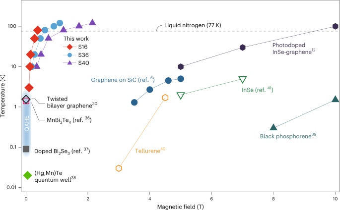
The diagram summarizes magnetic fields (below 10 T) and temperatures that realize quantized Hall conductance in several typical systems reported recently. Data from three samples (devices S16, S36 and S40) in this work are included.
In conclusion, we have demonstrated a hybrid system of graphene–CrOCl, in which an exotic QHE phase was observed thanks to the peculiar gate tunable interfacial coupling. At finite magnetic fields and constant Deff, a crossover from fan-like to cascade-like Landau quantization is seen. Also, in the D–B space, unlike in conventional D-independent ones, the LLs in the SIC–QHE phase exhibits a parabolic dependence between B and Deff in a wide effective doping range from 0 to 1013 cm−2, with a Landau quantization of a ν = ±2 plateau starting from as low as sub-100 mT below 10 K, and remains quantized at ~350 mT at liquid nitrogen temperature. Our theoretical analysis self-consistently attributes the physical origin of this observed phenomenon to the formation of a long-wavelength charge order in the interfacial states in CrOCl and a subsequent band reconstruction in graphene. Our findings seem to open a new door to engineering the QH phase, and may shed light on the future manipulation of quantum electronic states via interfacial charge coupling, such as to construct novel topological superconductors, and to build quantum metrology standards.
- Coinsmart. Europe’s Best Bitcoin and Crypto Exchange.Click Here
- Platoblockchain. Web3 Metaverse Intelligence. Knowledge Amplified. Access Here.
- Source: https://www.nature.com/articles/s41565-022-01248-4