
The ability to run the same structural tests at different points in the product lifecycle could catch more failures.

By Ash Patel and Karthik Natarajan
Chip testing has become increasingly complex due to the number of variables impacting designs – from design size and complexity, to high transistor counts on advanced technology nodes, to 2.5D/3D packaging, to manufacturing variability. All of these combine to make testing today’s chips and packages more complicated than ever before. The number of test patterns required has grown from a few thousand to a few hundred thousand, resulting in increased test time and test cost on Automated Test Equipment (ATE). In parallel, the very definition of “chip test” has expanded beyond manufacturing and now includes in-field. Aging effects and silicon degradation over time, especially in safety-critical applications, must be detected for chips in active use in end systems. The combination of these factors requires new solutions that provide test results much faster and at multiple points in the silicon lifecycle – from post-silicon validation (PSV) of prototypes through chip manufacturing test on automatic test equipment (ATE), system-level test (SLT) of the assembled board containing the chip, and onto in-system test (IST) of the assembled product in the field.
As show in in figure 1 below, some parts which pass structural test at ATE stage, fail at the SLT step validating the need for structural testing at SLT stage. One reason for this SLT fail could be the difference between the ATE & SLT testing environments. Having the ability to run the same structural tests (ex. scan or memory BIST) on ATE & SLT could catch these failures and provide the much-needed diagnosis capability. The main reason for not running ATE structural vectors on SLT is the lack of test access mechanisms (GPIOs) at SLT which are used in ATE. This lack of test access further validates the strong need for a solution that would enable structural test patterns to be portable from PSV to ATE to SLT to IST stages.

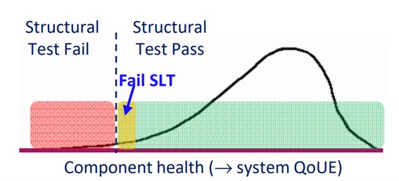
Fig. 1: Test escapes from ATE detected at SLT.
Synopsys Silicon Lifecycle Management (SLM) High Speed Access & Test IP (HSAT) combined with Synopsys Test Adaptive Learning Engine (ALE) software enables the portability of structural test content from PSV to ATE to SLT & IST as shown in figure 2. The HSAT IP solution reuses standard HSIOs interface (ex. PCIe or USB) to enable test, debug, and monitoring data to be accessed in and out of an SoC at gigabit data rates. ALE packetizes and depacketizes scan data for transmission over the interface through the HSAT IP. ALE reads in Standard Test Interface Language (STIL) to packetize the content that would be sent over the HSIO interface to the HSAT IP which in turn drives the scan and tap network. ALE also compares the received responses from the chip with the expected responses and if there are differences generates the appropriate failure logs for diagnosis. The unique aspect of this solution is that it uses the native functional protocol of the HSIO interface, thereby scaling efficiently as the protocol scales for functional needs. This also enables the portability of content across the various platforms (PSV, ATE, SLT & IST).


Fig. 2: Scan patterns can be applied at any stage via HSAT solution.
The HSAT solution also solves the need for higher bandwidth to test designs. Many of today’s SoCs have high-speed interfaces such as USB & PCIe readily available. A PCIe Gen 6 standard is rated at 64 giga transfers per second on a single lane. Considering a worst-case scenario of 50% protocol overhead, a single lane PCIe Gen 6 can provide a bandwidth that is equivalent to 160 GPIOs running at 200 Mhz. Similarly, a fourth generation of the ubiquitous Universal Serial Bus (USB) clocks at 40 gigabits per second which is sufficient bandwidth for many chips. Architecting the DFT to leverage these HSIO interfaces significantly reduce the test time and test cost. When a chip is being tested during WS/FT, it is typically not actively communicating with other chips. Using its functional interfaces as part of the testing process is a logical and very effective approach. To satisfy the requirement of unified testing across the full silicon lifecycle, the testing must be flexible as well as fast.
Using functional HSIO to perform high-bandwidth test is made much easier with Synopsys HSAT IP. Designers can instantiate HSAT IP into their SoCs to seamlessly connect chip DFT infrastructure to interfaces such as PCIe, USB, Serial Peripheral Interface (SPI) and Mobile Industry Processor Interface (MIPI). This is much higher performance than using GPIO for test and it avoids having to allocate GPIO pins for test purposes. In fact, no additional pins are required at all. The connection to the HSIO interface is made using a configurable Arm AMBA AXI interface and a FIFO suitable for the design’s DFT approach. A bypass mode to use GPIO pins is available. The connection to the DFT logic is flexible in order to accommodate different architectures, including configurable scan chain, compression, and JTAG Test Access Port (TAP) support. These capabilities provide maximum interoperability across many different types of SoCs.

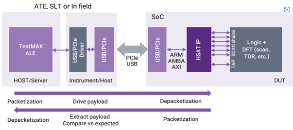
Fig. 3: Block diagram of HSAT+ALE solution.
In summary, chip test methodology is undergoing major changes in the manufacturing process. Traditional methods using low-speed interfaces are limited to ATE stage. The Synopsys solution with HSAT IP and ALE software leverages existing functional HSIO such as PCIe and USB to speed up SoC test while adding no pins. The solution scales as new generations of HSIO standards become available. High-bandwidth testing is possible from wafer test to in-field monitoring, spanning the entire silicon lifecycle. The same flow works for PSV, ATE, SLT, and IST allowing for scan pattern portability. Repeating manufacturing tests in the field further provides early visibility into SoC performance degradation over the chip’s lifetime enabling a more complete Silicon Lifecycle Management (SLM) solution.
For more information, visit https://www.synopsys.com/solutions/silicon-lifecycle-management/high-speed-access-and-test.html and https://www.synopsys.com/implementation-and-signoff/test-automation/testmax-ale.html.
Karthik Natarajan is the director of solution engineering for test at Synopsys.
Ash Patel
(all posts)
Ash Patel is director of product marketing at Synopsys.
- SEO Powered Content & PR Distribution. Get Amplified Today.
- Platoblockchain. Web3 Metaverse Intelligence. Knowledge Amplified. Access Here.
- Source: https://semiengineering.com/scan-pattern-portability-from-psv-to-ate-to-slt-to-ist/